Beyond Flat: Why 200+ Layer 3D NAND is Reshaping Storage

How vertical stacking technology is revolutionizing SSD storage capacity, performance, and efficiency.
Remember the not-so-distant past of storage juggling? Maybe it was deciding which games to uninstall on your early SSD, watching a massive video render grind your system, or simply hitting the capacity wall far sooner than expected. That constant awareness of storage limits was, frankly, a bottleneck on creativity and productivity.
For years, the industry masterfully shrank components on traditional 2D (planar) NAND flash. It was an incredible feat of engineering, giving us the first taste of solid-state speed. But like trying to fit a growing city onto a fixed plot of land, building outwards eventually hits fundamental limits. Shrinking transistors further became exponentially difficult and costly – a challenge known as lithography scaling. Performance gains started to level off. We needed a new dimension.
Adding a Z-Axis: The Birth of 3D NAND
The elegant solution? Build up. 3D NAND technology stacks memory cells vertically, layer upon layer, much like constructing a skyscraper instead of endless single-story buildings.
This vertical approach was revolutionary. It allowed manufacturers to dramatically increase storage density (how much data fits in a given physical space) without relying solely on shrinking individual components to near-impossible sizes. Early 3D NAND, with 32 or 64 layers, already offered significant bumps in capacity and helped bring down the cost per gigabyte, making SSDs mainstream.
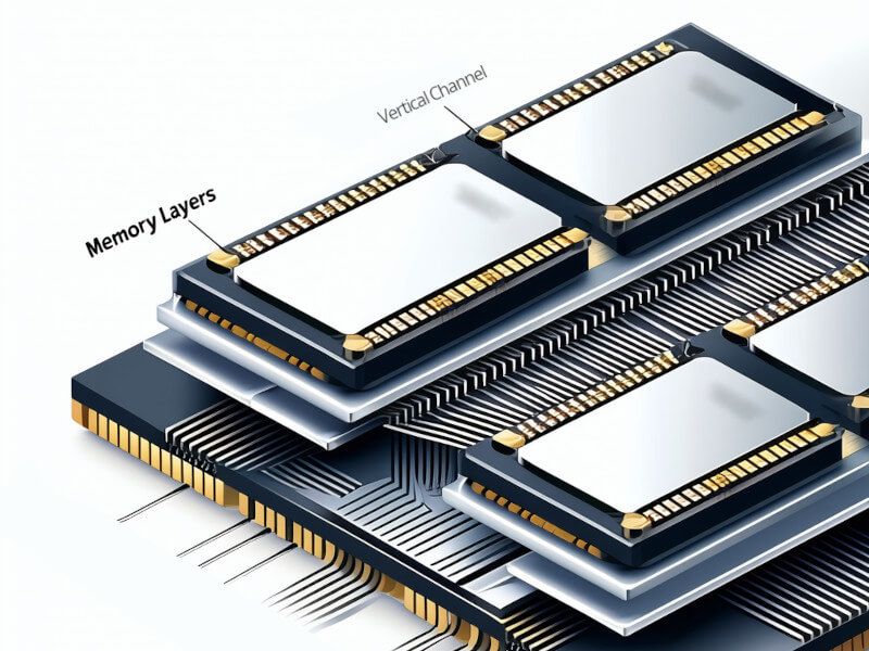
The Intricate Dance of Stacking Layers
What followed was an intense period of innovation – the "layer race." We saw jumps from 64 to 96, then 128, 176 layers, and beyond.
Don't mistake this for simply piling silicon pancakes. Each step required overcoming immense engineering hurdles:
- Precision Etching: Creating incredibly deep, narrow vertical channels (with high aspect ratios) through the entire stack to connect the cells.
- Material Consistency: Ensuring atomic-level uniformity when depositing the various material layers across the whole wafer.
- Stress Control: Managing the immense physical stresses inherent in these complex, multi-layered structures.
Achieving this level of precision at nanoscale, repeated billions of times per chip, is truly mind-boggling.
Crossing the 200-Layer Milestone: What It Unlocks
Now, the industry is routinely manufacturing and shipping NAND with over 200 layers, and pushing towards 300. This isn't just an incremental number increase; it signifies a maturity in the technology that translates to tangible benefits you can feel:
- Massive Capacity Becomes Normal: Higher stacks mean more gigabytes (or terabytes) per chip. This is how we get readily available 4TB and 8TB NVMe SSDs that fit in the palm of your hand. The direct benefit? Less worrying about space, more doing. Keep your OS, apps, huge game installs, RAW photo libraries, and 4K/8K video projects all on fast, primary storage. It’s about removing friction from your workflow.
- Unleashing Interface Speed: While capacity is key, these denser NAND packages, often combined with architectural improvements (like more internal data pathways or "planes"), are essential for truly exploiting modern high-speed interfaces. Early SSDs saturated SATA III (~550 MB/s). 200+ layer NAND helps drive PCIe 4.0 and 5.0 NVMe SSDs to blistering speeds – think 7,000 MB/s, 10,000 MB/s, and even faster. This translates directly to near-instant boot times, rapid application loads, seamless high-bitrate video scrubbing, and dramatically faster game level loading.
- Improved Power Efficiency: Generally, packing more data into the same silicon footprint improves power efficiency per gigabyte. Less energy is consumed for storing and accessing data. This means tangible battery life gains in laptops and potentially lower energy bills and heat output for desktops and servers.
- The Economics of Density: A primary driver for stacking higher is manufacturing cost-efficiency. By fabricating more storage capacity on a single expensive silicon wafer, the cost per gigabyte tends to decrease over time (even if the absolute drive cost is high initially for cutting-edge tech). This makes larger, faster drives more accessible.

Living in the Vertical Era
So, what does this highly stacked NAND mean for you right now?
It means NVMe drives that barely pause for breath when loading complex game worlds or large datasets. It means laptops that can hold enormous media libraries while sipping power. It means workstations that chew through demanding tasks without the storage being the bottleneck.
The evolution to 200+ layer 3D NAND isn't just about chasing bigger numbers. It's about fundamentally improving the performance, capacity, and efficiency of the storage that underpins almost everything we do with our computers. The data skyscrapers are built, and they’re enabling a faster, less constrained digital experience than ever before.